

APCSCRM 2023
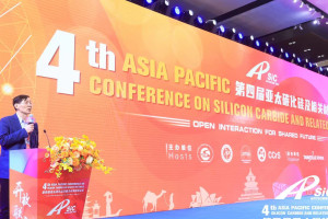
The Asia-Pacific Conference on Silicon Carbide and Related Materials, APCSCRM has been held in Beijing from November 8th to 10th, 2023.The Asia-Pacific International Conference on Silicon Carbide and Related Materials (APCSCRM) focuses on the multidisciplinary theme of wide-bandgap semiconductors (silicon carbide, gallium nitride, gallium oxide, aluminum nitride, diamond, etc.) materials and devices such as silicon carbide, and has now become a broad-based conference in the Asia-Pacific region. A high-level forum that places equal emphasis on the bandgap semiconductor industry and academia, driving the integrated development of silicon carbide and other wide bandgap semiconductor industries and academia in the Asia-Pacific region.
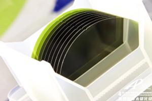
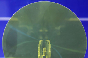
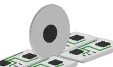
Silicon Crabide wafer for Semi-conductor industry
Moresuperhard have participant this conference and learned a lot of knowledge from APCSCRM.Now ,Let's learn some core content together.
1.Development difficulties of silicon carbide wafer
Due to the global shift to electric vehicles and the goal of actively achieving carbon neutrality, the SiC power semiconductor market is expanding rapidly, and the growth rate of the SiC epitaxial wafer market is far faster than that of the semiconductor materials market. The demand for SiC epitaxial wafers from electric vehicles will also increase rapidly. In order to meet the needs of electric vehicles, costs need to be reduced and quality improved. 8-inch is one of the key items to reduce costs.
2.The main preparation process of silicon carbide crystal
At present, the mainstream methods of growing silicon carbide include physical vapor transport method (PVT method), liquid phase method, and high-temperature vapor phase chemical deposition(HPCVD) method.
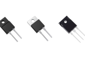
3.Application of silicon carbide in power devices
Devices made of SiC have performance advantages such as high efficiency and fast switching speed. They can significantly reduce product energy consumption, improve energy conversion efficiency and reduce product size. They are ideal materials for manufacturing high-voltage power devices. Currently, SiC devices are widely used in new energy vehicles, charging piles, smart grids, photovoltaic inverters, wind power and other fields.
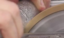
4.Research on cutting, grinding and polishing of silicon carbide substrates
At present, the mainstream method for cutting silicon carbide is mortar wire cutting (free abrasive wire cutting). Mortar wire cutting (free abrasive wire cutting) refers to the reciprocating high-speed movement of the cutting wire during the processing process, and sprays in the crystal rod and the cutting line. Cutting fluid, high-speed moving cutting wire brings abrasives to the processing area to achieve material cutting.
The purpose of grinding is to remove the tools marks and surface damage layer on the surface of SiC slices caused during the cutting process. Due to the high hardness of SiC, high-hardness abrasives (such as boron carbide or diamond powder) must be used to grind the crystal surface of SiC slices during the grinding process. Grinding can be divided into rough grinding and fine grinding according to different processes.
Ultra-precision polishing is a very critical link in the SiC surface processing process, among which chemical mechanical polishing (CMP) technology is currently the most effective method to achieve global planarization of SiC wafers. CMP is a process that achieves surface material removal and planarization of workpieces through the synergistic effect of chemical corrosion and mechanical wear.
Summarize
The successful holding of the 4th Asia-Pacific International Conference on Silicon Carbide and Related Materials (APCSCRM 2023) not only injected new impetus into academic research and technological innovation in the field of wide-bandgap semiconductors in the Asia-Pacific region, but also provided new opportunities for the development of related industries. and cooperation space to further strengthen international exchanges and cooperation and promote academic research, technological progress and industrial upgrading of silicon carbide and other wide-bandgap semiconductor industries in the Asia-Pacific region.
Evaluation of circuit board quality and process improvement requires slicing as a basis for objective inspection and judgment. Slice analysis using metallographic equipment is an important means to check the thickness of PCB/PCBA internal circuits, number of layers, through hole aperture size, through hole quality observation, PCB/PCBA solder joint cavity, interface bonding status, and wetting quality evaluation.
Moresuperhard offers resin diamond cutting discs and metal diamond cutting discs specifically for cutting in the glass industry. It can be used to cut glass optical devices such as quartz glass, K9 glass, coated glass, etc. It can also be used to cut various glass tubes, glass spouts, high borosilicate glass tubes, capillary glass tubes, quartz glass, and crystallized glass.
Add: Zhongyuan Rd, Zhongyuan District, Zhengzhou, 450001, Henan, China
Tel: +86 17700605088


