
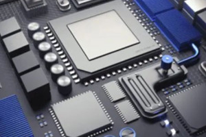
Modern microelectronics technology is developing rapidly, and electronic systems and equipment are developing in the direction of large-scale integration, miniaturization, high efficiency and high reliability. The increase in the integration of electronic systems will lead to higher power density, as well as an increase in the heat generated by the overall operation of electronic components and systems, so effective packaging must address the heat dissipation of electronic systems.
The requirements of packaging substrate materials are: high resistivity, high thermal conductivity, low dielectric constant, dielectric loss, good thermal matching with silicon and gallium arsenide, high surface flatness, good mechanical properties and easy industrial production. The general packaging substrate has Al2O3 ceramic, SiC ceramic, AlN material.
However, the thermal expansion coefficient and dielectric constant of Al2O3 are relatively high compared with Si single crystals, and the thermal conductivity is not high enough, resulting in the Al2O3 ceramic substrate is not suitable for use in high frequency, high power, and very large scale integrated circuits.
With high thermal conductivity ceramic substrate materials SiC, AlN, SI3N4, diamond gradually entered the market. The thermal conductivity of SiC ceramics is very high, and the higher the purity of SiC crystal, the higher the thermal conductivity. The biggest disadvantage of SiC is that the dielectric constant is too high and the dielectric strength is low, so it limits its high-frequency application and is only suitable for low-density packaging.
AlN material has excellent dielectric properties, stable chemical properties, especially its thermal expansion coefficient and silicon better match, so it can be used as a promising semiconductor packaging substrate material. However, the thermal conductivity is low, and with the increasing demand for heat dissipation in semiconductor packaging, AlN materials also have certain development bottlenecks.
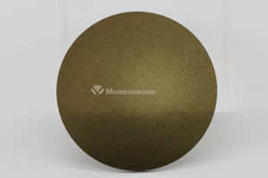
Final diamond stand out, diamond has good comprehensive thermal physical properties, its thermal conductivity at room temperature is 700 ~ 2200W/ (m·K), thermal expansion coefficient is 0.8×10⁻⁶/K, in semiconductor, optics and other aspects have many excellent properties, but a single diamond is not easy to make into packaging materials, and the cost is high.
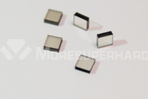
According to the mixing rule, diamond/metal matrix composites prepared by adding diamond particles to Ag, Cu, Al and other high thermal conductivity metal substrates are expected to become a new type of electronic packaging materials with low thermal expansion coefficient and high thermal conductivity. According to the excellent electrical conductivity and high thermal conductivity of copper, diamond/copper composite material was developed as the substrate material for electronic packaging, and it was confirmed that diamond/copper composite material has better plating and weldability, which meets the performance requirements of low thermal expansion coefficient and high thermal conductivity of electronic packaging substrate material. The density is smaller and the weight is lighter, so the diamond/copper composite material with diamond as the reinforcement phase and copper as the matrix material can be used for chip packaging, which can improve the performance of electronic equipment system and help to reduce the weight of equipment.
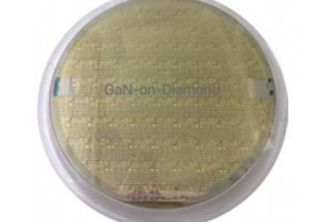
Diamond can also be used as a substrate for GaN power devices to help them dissipate heat for higher frequencies and higher power. In the past decade, many developed countries have invested a lot of money to promote the growth of diamond on the back of GaN devices by chemical vapor deposition (CVD), and vigorously promote the development of diamond-based GaN devices. GaN on diamond substrate has 3 times higher transistor power density than GaN on silicon carbide substrate. Diamond substrate material can greatly reduce the thermal variable resistance, so that GaN equipment can operate normally under higher power density conditions, but also greatly reduce the cost of equipment, size, weight and energy supply.However, due to the high price, the application of gallium nitride devices on diamond substrates is limited to the fields of national defense and aerospace.
Studies have found that:Diamond-based semiconductors can be the substrate for any wafer Which called SOD(silicon on diamond).
At present, the application of diamond semiconductors in new materials, new devices and new technologies is in a stage of rapid development, and the world is stepping up the research and development of diamond in the semiconductor field. Its continuous innovation and development has also brought broader application prospects for all walks of life.
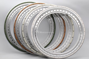
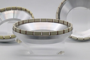
MORESUPERHARD has been in diamond industry for many years, for diamond substrate we can provide suitable grinding and polishing solutions.
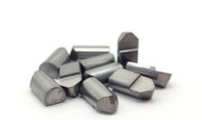
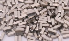
With tungsten carbide prices soaring 200%+, PCD & CBN become cost-effective alternatives. Moresuperhard provides high-quality PCD/CBN blanks, grinding wheels & grinders to help manufacturers reduce costs and improve efficiency.
Learn the technical characteristics, advantages, disadvantages and applicable working conditions of standard TSP and nickel-based coated TSP. Compare their performance differences and master the selection skills for drilling, cutting and grinding scenarios.
Add: Zhongyuan Rd, Zhongyuan District, Zhengzhou, 450001, Henan, China
Tel: +86 17700605088