
The relationship between silicon carbide and semiconductor materials
The silicon carbide production process includes the preparation of material end substrates and epitaxy, the design and manufacture of subsequent chips, and then the packaging of devices, and finally flows to the downstream application market. Among them, the substrate material is the most challenging link in the silicon carbide industry.

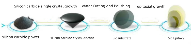
The main steps of silicon carbide substrate preparation
The silicon carbide substrate preparation process mainly includes raw material synthesis, silicon carbide crystal growth, ingot processing, ingot cutting, cutting piece grinding, grinding piece polishing, polishing piece cleaning, etc.
Among them, the key and difficult points of preparation are mainly the crystal growth, cutting, grinding and polishing links, which are the key points and difficulties in the entire substrate production process, and become the bottleneck that limits the yield rate and production capacity of silicon carbide.
1.Crystal Growth
Crystal growth is slow
The growth rate of silicon carbide is only 0.3-0.5mm/h, and the maximum crystal length can only reach 2-5cm, which is quite different from silicon-based substrates. And as the size of silicon carbide crystals expands, the difficulty of its growth process increases geometrically
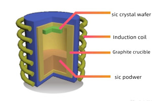
Low yield rate of black box operation
The core parameters of silicon carbide substrates include micropipe density, dislocation density, resistivity, warpage, surface roughness, etc. The production process is completely completed in a high-temperature sealed graphite cavity. It is necessary to arrange the atoms in the closed high-temperature cavity in an orderly manner to complete the crystal growth and control the parameter indicators at the same time. It is very dependent on the manufacturer's process experience and is prone to various defects and other problems. The crystal growth process is difficult, the yield rate is low, and the output is small.
Polymorph inclusion problem
There are many types of silicon carbide crystal structures, but only a few of them are the required materials. It is difficult to control impurities, and it is easy to produce polycrystalline inclusions, which reduces the qualified rate of products.
2.Cutting, Grinding and Polishing
After the silicon carbide crystal is prepared, it needs to be cut into thin slices with a thickness of no more than 1mm along a certain direction, and ground with diamond abrasive fluids of different particle sizes to remove knife marks and metamorphic layers and control the thickness before CMP Polishing for global planarization followed by final cleaning.
Difficulties in cutting, grinding and polishing: Since silicon carbide is a brittle material with high hardness, it has serious problems such as warping and cracking during processing, and the loss is huge. Under the traditional reciprocating diamond-bonded abrasive multi-wire cutting method, the overall material The utilization rate is only 50%. After polishing and grinding, the cutting loss ratio is as high as 75%, and the usable part ratio is relatively low.
Slicing of SIC single crystal
As the first process in the silicon carbide single crystal processing process, the performance of the slice determines the processing level of subsequent thinning and polishing. The slicing process is easy to produce cracks on the surface and sub-surface of the wafer, which increases the fragmentation rate and manufacturing cost of the wafer. Therefore, controlling the crack damage on the surface of the wafer is of great significance to promote the development of silicon carbide device manufacturing technology.
How to optimize the slice quality of silicon carbide single crystal?
Surface crack damage is closely related to slice quality. The epitaxial growth on the silicon carbide substrate material, the device manufacturing process and the device performance are all related to the crystal orientation. In order to avoid brittle cracks in wafers caused by orientation sensitivity during slicing, crystal orientation detection is required before slicing silicon carbide ingots. Silicon carbide ingots are generally grown on the SiC { 0001} plane, and cutting along the SiC crystal plane parallel to the growth direction of the ingot can effectively reduce the through-thread dislocation density on the slice surface and improve the slice quality.
Thinning of silicon carbide wafers
The thinning of silicon carbide slices is mainly achieved by grinding and lapping
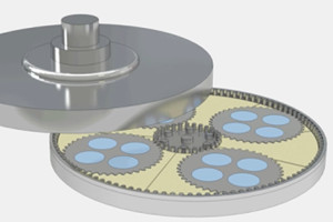
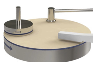
1.Grinding
The most representative form of wafer grinding is self-rotation grinding. While the wafer is self-rotating, the spindle mechanism drives the grinding wheel to rotate, and at the same time the grinding wheel is fed downwards to realize the thinning process.
2.Lapping
The lapping process can be divided into single-side and double-side grinding, and single-side and double-side grinding technologies for small-sized silicon carbide wafers have been developed one after another. When grinding the surface of silicon carbide slices, the abrasive used is usually boron carbide or diamond, which can be divided into rough grinding and fine grinding. Coarse grinding is mainly to remove the knife marks caused by slicing and the metamorphic layer caused by slicing, and the abrasive grains with larger particle sizes are used. The purpose of fine grinding is to remove the surface damage layer left by coarse grinding, improve the surface roughness, and use finer abrasive grains.
Main Factors Affecting Thinning Effect
The study found that the wafer material removal rate in the thinning process is closely related to abrasive particle size, density, grinding disc rotation speed, grinding pressure and other factors. The higher the hardness of the abrasive grains in the slurry, the larger the grain size, and the greater the surface roughness of the processed wafer. Too hard grinding disc will damage and pollute the surface of the workpiece, soft grinding disc can allow more sliding movement of the abrasive, the surface finish after processing is high, but the flatness is low.
Polishing of silicon carbide wafers
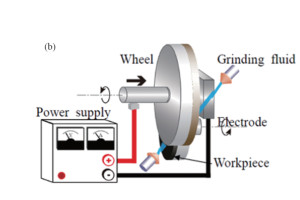
The polishing process of silicon carbide wafers can be divided into rough polishing and fine polishing, and rough polishing is mechanical polishing.The main research direction of the fine polishing process of silicon carbide single crystal is to develop a composite process that combines chemical and mechanical synergies. The chemical synergy methods mainly include electrochemistry, magnetorheology, plasma, photocatalysis, etc. The mechanical synergy methods mainly There are ultrasonic-assisted, mixed abrasive and fixed abrasive polishing methods.
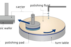
Key factors and development trends affecting CMP
Polishing results are optimized when the mechanical and chemical effects of CMP are balanced. The polishing effect of CMP is mainly affected by three parameters: process parameters, polishing liquid, and polishing pad. Polishing fluid and polishing pads are the main consumables in CMP, and controlling and optimizing their properties to ensure repeatable polishing efficiency is critical for process stability. Improving the polishing liquid and developing a polishing pad with self-catalysis is the research direction of CMP consumables in the future
With tungsten carbide prices soaring 200%+, PCD & CBN become cost-effective alternatives. Moresuperhard provides high-quality PCD/CBN blanks, grinding wheels & grinders to help manufacturers reduce costs and improve efficiency.
Learn the technical characteristics, advantages, disadvantages and applicable working conditions of standard TSP and nickel-based coated TSP. Compare their performance differences and master the selection skills for drilling, cutting and grinding scenarios.
Add: Zhongyuan Rd, Zhongyuan District, Zhengzhou, 450001, Henan, China
Tel: +86 17700605088