

DC Arc Jet CVD Wafer and Microwave Plasma CVD (MPCVD) Wafer are the two mainstream industrial technologies for mass-producing high-performance CVD synthetic diamond wafers. Their core divergence originates from distinct plasma gas activation mechanisms, which lead to obvious gaps in deposition speed, crystal purity, achievable thickness, finished wafer size and applicable industrial scenarios.
Direct Current Arc Jet Chemical Vapor Deposition (DC Arc Jet CVD) and Microwave Plasma Chemical Vapor Deposition (MPCVD) are the two dominant synthesis technologies for producing high-quality synthetic diamond wafers. The fundamental difference lies in their plasma excitation methods, which directly dictate growth rate, purity, crystalline morphology, and downstream industrial applications.
This article systematically sorts out their working principles, performance indicators, product characteristics and downstream matching fields, providing clear material selection reference for semiconductor thermal management, optical engineering, ultra-precision machining and quantum technology industries.
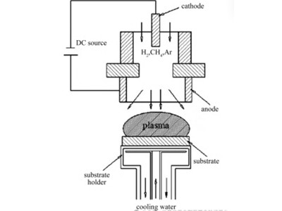
Direct Current Arc Jet Chemical Vapor Deposition (DC Arc Jet CVD) relies on direct current discharge inside a cylindrical channel to heat mixed carbon source gas, generating ultra-high-temperature plasma jet with core temperature up to tens of thousands of Celsius degrees. The high-speed plasma stream is sprayed onto the substrate surface through a dedicated nozzle.
This process delivers ultra-high plasma density and ionization rate, producing massive carbon-containing active radicals to support extremely fast diamond deposition. However, the built-in metal electrodes will continuously erode during long-term operation, introducing metallic impurities into the diamond layer; besides, the intense jet reaction makes the growth environment less gentle and harder to fine-tune microscopically.
DC Arc Jet CVD: Gas is heated by a DC discharge in a cylindrical channel, forming a high-temperature (core temperatures up to tens of thousands of degrees Celsius) high-velocity plasma jet that is ejected through a nozzle onto the substrate. High plasma density and ionization degree yield extremely high concentrations of active species and thus high deposition efficiency. However, electrodes can introduce metallic impurities, and the process is relatively violent.
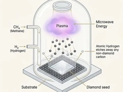
Microwave Plasma Chemical Vapor Deposition (MPCVD) adopts electrode-free microwave excitation mode. Microwave energy is injected into the sealed reaction chamber to form a stable, spherical plasma field without any metal electrodes contacting the plasma area.
The plasma environment maintains outstanding uniformity and cleanliness, with fully adjustable core parameters including microwave power, chamber pressure, gas mixing ratio and substrate spacing. The stable, pollution-free reaction environment supports uninterrupted long-time epitaxial growth, which is the core advantage for manufacturing ultra-high-purity, low-defect diamond wafers.
MPCVD: Microwave energy creates a stable “plasma ball” inside the reactor chamber without metal electrodes, resulting in a clean, highly controllable plasma. Gas activation is uniform, and parameters (power, pressure, gas ratios, substrate distance) can be precisely adjusted, enabling long-term stable growth of high-quality diamond.
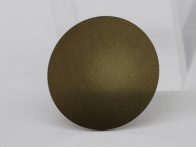
DC Arc Jet CVD products focus on cost efficiency, ultra-thick structure and large-area supply, widely adopted in heavy industrial manufacturing and medium-performance thermal dissipation fields:
DC Arc Jet CVD wafers are better suited for industrial thick-film and cost-sensitive applications: High-power electronics heat sinks/spreaders, infrared optical windows and domes; Tool coatings, dressing tools, wear parts; Large polycrystalline diamond plates (thermal management, machining).
MPCVD ultra-clean crystal characteristics support cutting-edge industries with strict impurity and defect control standards:
MPCVD wafers dominate high-purity, high-precision fields: Electronic-grade single-crystal diamond substrates (power devices, RF, quantum sensing/computing); Gem-quality lab-grown diamonds, optical-grade windows; High-precision heat sinks, semiconductor thermal management, optoelectronic and quantum devices.
MORESUPERHARD (More SuperHard Products Co., Ltd.) is a global integrated supplier of superhard materials and precision machining solutions, owning a complete product matrix covering all mainstream CVD diamond forms, including CVD synthetic diamond plates, PCD/PCBN/MCD/CVD blanks and customized diamond components.
MORESUPERHARD (More SuperHard Products Co., Ltd.), a supplier of superhard materials and precision machining solutions, offers a product line covering various CVD diamond forms, including CVD synthetic diamond plates, PCD/PCBN/MCD/CVD blanks, and more.
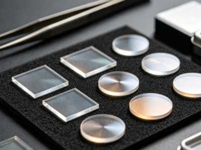
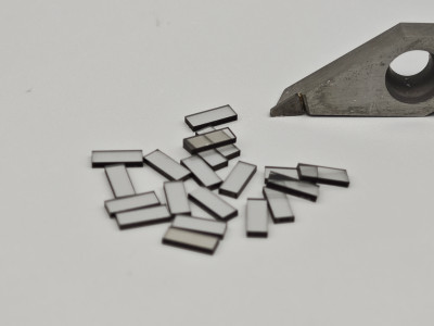
Its CVD diamond plates feature high transmission, excellent thermal and chemical stability, low surface roughness, superior cutting-edge quality, higher wear resistance, and thermal conductivity 50% higher than PCD. Thicknesses range from 0.3 mm to 3 mm with flexible sizes (e.g., 1×1×1 mm and larger).
By combining the fast thick-film strengths of DC Arc Jet CVD and ultra-high-purity merits of MPCVD, MORESUPERHARD provides targeted customized materials for diverse client demands:
Beyond raw diamond materials, the company supplies supporting diamond grinding wheels, precision surface polishing and finished part machining services, forming a closed-loop industrial chain from diamond synthesis to finished component delivery.
By integrating the high-speed thick-film advantages of DC Arc Jet CVD with the high-purity strengths of MPCVD, MORESUPERHARD can deliver tailored solutions: cost-effective thick-film CVD products for industrial tools and thermal management, and higher-quality CVD wafers/plates for semiconductor, optical, and precision machining needs. The company also provides complementary diamond grinding wheels, polishing, and processing services, forming a complete support chain from materials to applications.
DC Arc Jet CVD and MPCVD are not competitive alternatives with absolute superiority or inferiority, but two complementary technical routes built on core trade-offs: deposition speed vs crystal purity, large thick-film manufacturing vs ultra-precise high-purity crystal growth. Enterprises should select corresponding diamond wafer solutions based on clear indicators including production efficiency limit, impurity threshold, target material thickness and comprehensive cost budget.
DC Arc Jet CVD and MPCVD are not simply superior or inferior to each other, but represent a strategic trade-off between speed and purity, scale and precision. The choice depends on the specific requirements of the end application regarding growth efficiency, impurity control, thickness, and cost.
With continuous breakthroughs in 8-inch and above large-size CVD diamond wafer technology, plus the maturing supporting processing capacity of leading manufacturers like MORESUPERHARD, the two core CVD diamond manufacturing technologies will jointly accelerate the large-scale popularization of diamond functional materials across thermal management, advanced semiconductors, precision optics and ultra-precision machining industries.
With ongoing advances in large-size wafer technology (especially 8-inch and beyond) and the refinement of CVD diamond products and supporting processing by companies such as MORESUPERHARD, these two core technology routes will jointly drive broader applications of diamond materials in thermal management, semiconductors, optics, precision machining, and beyond.

Custom electroplated, sintered & CVD‑enhanced diamond rotary dressers for aerospace, semiconductor, new‑energy vehicle, robotics. High profile accuracy & long service life.

What Can a CVD Diamond Do? Complete industrial chain from CVD diamond plate, precision grinding to CVD / PCD cutting tool manufacturing, Moresuperhard one‑stop superhard processing solution.
Add: Zhongyuan Rd, Zhongyuan District, Zhengzhou, 450001, Henan, China
Tel: +86 17700605088



